- Home
- About
- Products
- Gratings
- Grating Clamps
- S.S Linear Drain Channel
- S.S Drain Trap
- Cable Crane Trolly
- Paper Holder Dispensers
- Press Components With Die Development
- Manhole Cover
- Inspection Manhole Cover
- Slot Drain
- S.S Kitchen Drain Trap
- Railing And Straircases
- Flipbook
- Blog
- Contact
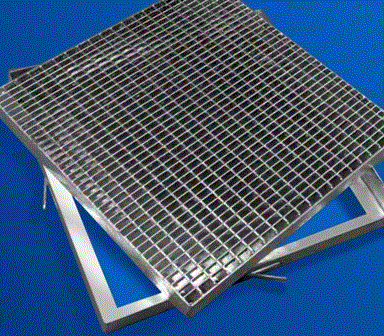
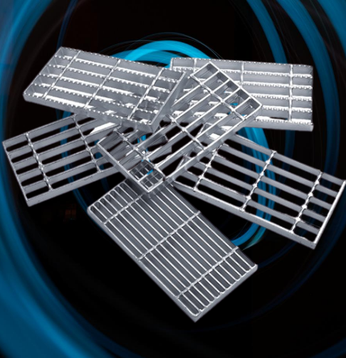
Platform grating, composed of several pieces of welded steel grating or press locked gratings are commonly installed in ships and industrial applications, such as refineries, power plants and offshore platforms.
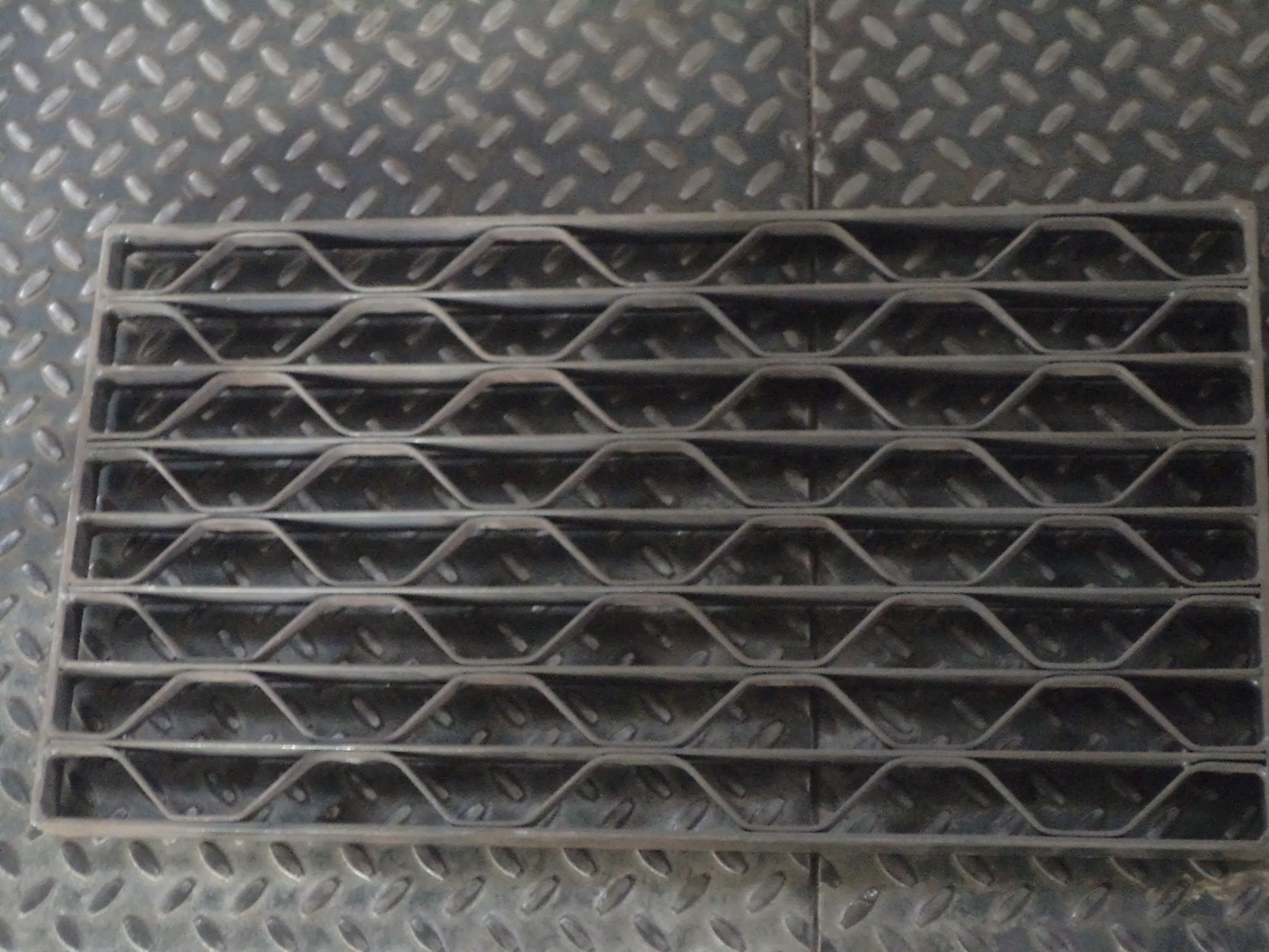
To meet all types of gratings requirement of clients. We develop Honeycomb(ZigZag) gratings with 3 dimensional varieties, Obtainable with us in a range of sizes, dimensions and modified forms, Mostly useful Walkway gratings where design is of Honey comb type Generally Construction includes Flat for frame :- 25/30/5/6/3 mm tk Flat for load bearing bar :- 12*3,25*3,25*5,30*5 mm in Zigzag form Cross bar & load bearing bar are both flats as per drg. sizes We can design same if you provide us Load carrying capacity & purpose of gratings. these offered gratings could be purchased from us in a number of dimensional provisions to select from. We guarantee delivering these gratings at the destination of our clients within the promised span of time
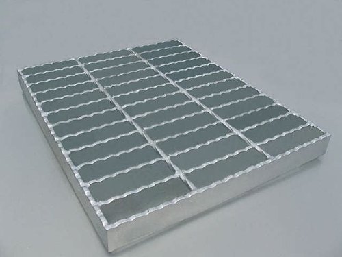
Being a well-established organization, we bring forth an excellent assortment of Hot Dip Galvanized Grating. Highly appreciated for its customized options, these gratings are basically used for decks on bridges, footbridges, and other similar places.
Painted Gratings suits for walkway use and storage rack floor stack for material storage use for both use Painted Gratings with synthetic /epoxy paint any colour of your choice Mesh size 25*30/30*50/40*50/30*100/40*100/25*100/any mesh size as per load carrying capacity we also help in best economical Grating to save cost on projects with indepth knowledge of gratings .
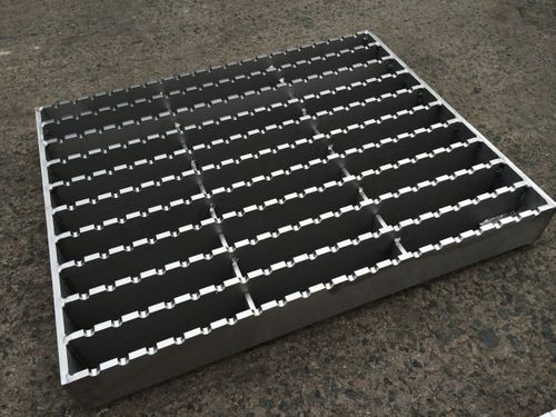
We can manufacture, export, supply and trade a supreme quality range of Intermesh Grating 40x100mm Mesh in Pune, Maharashtra, India, as per your need best economical way Image is of medium duty walkway Gratings. We can supply Intermesh 16/25/30/40/50/100 into 75/25/30/50/100 mm thickness of grate may be 20/25/30/32/40/50 mmtk..
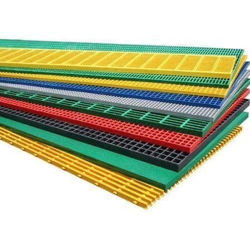
A new solution for Solar Panels. FRP Grating with low cost maintainence and very less weight. Quiet good for maintainence walkways. It reduces the weight of entire structure hence reducing the total weight on roof..
We are manufacturing serrated or anti-slip grating. The serrated top of the grating provides extra anti-slip protection in slippery environments, such as where oil spillages occur. Serrated gratings can also be the solution outdoors where snow and ice cause problems. The anti-slip gratings are available with round & Squae bars. Every other load bearing bar has been replaced with a round bar. This keeps the weight down and the requirement for a maximum mesh opening of 15 mm is satisfied. These gratings are specially designed for the offshore industry..
An embossing technique is used to fabricate surface-relief gratings into SiOtn2TiO2 dielectric, step-index, planar optical waveguides, fabricated using a sol-gel process. The influence that a pre-emboss bake cycle has upon the embossibility of the SiO2TiO2 sol-gel films is described. Through SEM evaluation, the embossed grating ruling profile and general appearance are shown to be strongly dependent upon the duration of the bake at 70 ° C. In addition, two embossing surface mechanisms, molding and stress-induced fracturing, are identified and correlated with the duration of the pre-emboss bake. Embossed waveguide gratings with a 0.52 μm period and 100–200 nm peak-to-trough depth were fabricated.
Our Best Products


